Insights
- Cadence offers an integrated 3D-IC design flow enabling seamless chiplet and multi-die integration.
- Their UCIe PHY, Controller, and VIP support combining diverse dies from various fabs and technologies.
- Solutions target automotive, data center, and other verticals requiring advanced packaging and performance optimization.
- Cadence’s tools address power, performance, area, timing closure, and complex simulation challenges.
- Comprehensive training and support resources help designers accelerate chiplet-based SoC development.
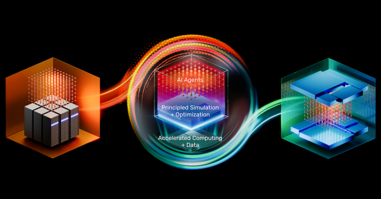
The advancement of 3D heterogeneous integration is transforming system-on-chip (SoC) design by enabling the seamless combination of multiple chiplets, including 2D and 2.5D dies, sourced from different fabs and packaging technologies. Cadence Design Systems leads this space by providing an integrated flow for chiplet and 3D-IC designs that serve automotive, data center, and various other industries.
The company’s Cadence UCIe PHY, Controller, and verification IP facilitate on-package mix-and-match chiplet configurations, allowing designers to optimize power, performance, and area (PPA) while achieving timing closure in multi-chiplet environments. Cadence’s comprehensive offerings cover design IP, verification, system-level analysis, and multi-die package implementation, backed by over 25 years of experience in advanced packaging.
These solutions address key challenges such as electromagnetic, thermal, and electromechanical simulations to ensure robust designs under diverse operating conditions. Through extensive educational resources and a supportive community, Cadence empowers engineers to accelerate innovation in disaggregated chip development, tackling physical constraints and cost issues at advanced semiconductor nodes effectively.