Category: tsmc
-
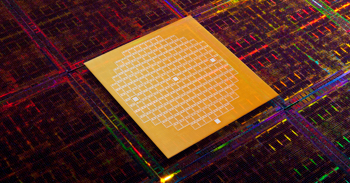
NVIDIA’s cuLitho Set to Boost Computational Lithography Performance
NVIDIA introduces cuLitho, a GPU-based computational lithography library, promising significant efficiency improvements for semiconductor manufacturing.
-
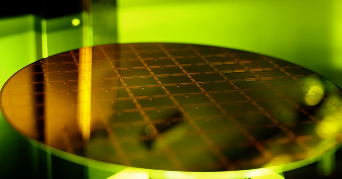
How AI is Turbocharging the World of Semiconductor Manufacturing
Key Highlights & Insights AI and accelerated computing are cutting down semiconductor design times from days to mere hours. Digital twin technologies simulate real-time factory processes to optimize production and safety. Generative AI models improve defect classification accuracy, saving costs and reducing wastage. Partnerships with giants like Samsung facilitate smarter, large-scale chip manufacturing. AI super…
-
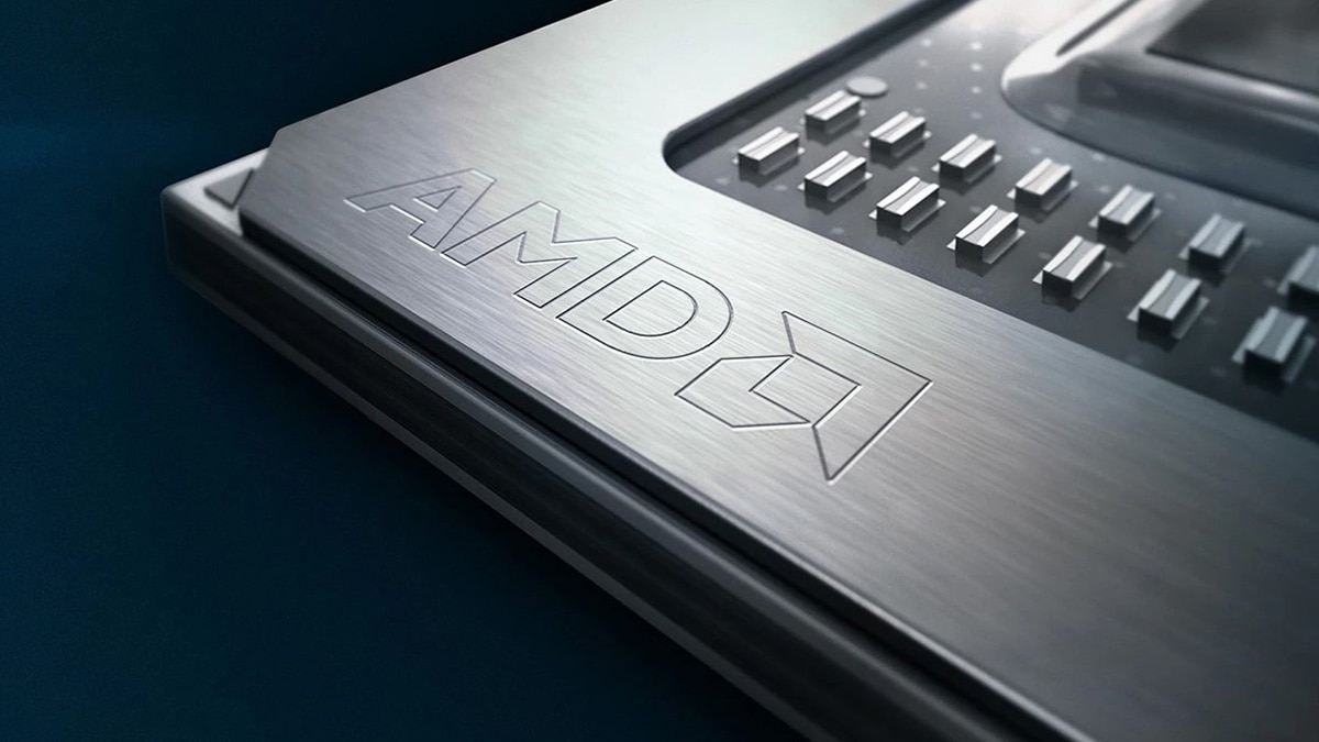
AMD Unveils Groundbreaking 2nm EPYC Venice CPU for AI and Data Center Revolution
Key Highlights & Insights AMD is pioneering the use of TSMC's 2nm process technology, setting a new industry standard for CPU manufacturing. The rollout of the Venice processor is a pivotal step in scaling AI infrastructures globally. Strategic geographical manufacturing diversification enhances AMD's global supply resilience. The forthcoming Verano processors aim to meet the rising…
-
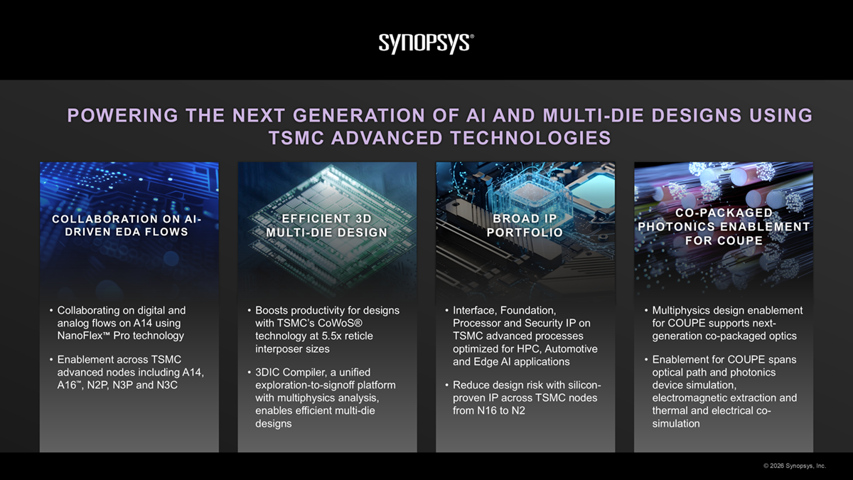
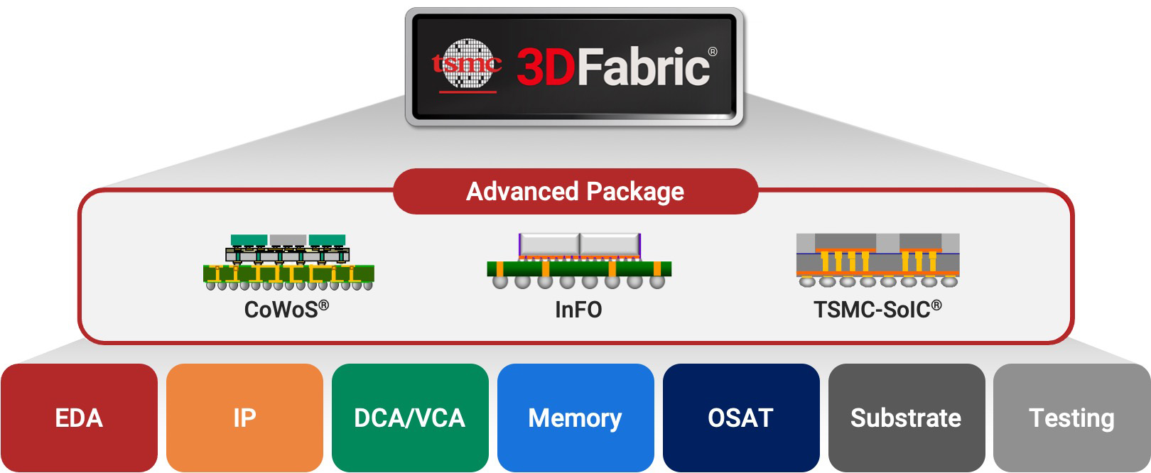
Synopsys and TSMC Unleash Groundbreaking AI Innovations with Next-Gen Silicon Technologies
Key Insights Synopsys and TSMC are pioneering AI systems through silicon-proven IP and certified EDA flows. The partnership has achieved groundbreaking technological milestones in silicon technology. Enhanced 3DFabric technologies have been unveiled, providing comprehensive integration for complex designs. Artificial intelligence features significantly in their solutions, boosting productivity and accelerating system time-to-market. The strategic expansion of…
-
TSMC Unveils A13 Process: Next-Gen AI and HPC Silicon Innovation
Insights: TSMC has unveiled its latest semiconductor process technology, the A13 node, at the 2026 North America Technology Symposium held in Santa Clara, California. This new process is a direct shrink of the previously announced A14 node, delivering a 6% reduction in chip area, which translates to more compact and efficient designs. These improvements primarily…
-
Cadence and TSMC Forge AI Chip Design Breakthroughs
Insights: Cadence and TSMC advance AI and HPC chip design with AI-driven automation and IP. Support for TSMC’s latest process nodes including N3, N2, A16, and upcoming A14 PDK. Enhanced 3D-IC design productivity enabled by Cadence solutions integrated with TSMC’s 3DFabric. New silicon-proven IP such as HBM4, LPDDR6/5X, PCIe 7.0, and Universal Chiplet Interconnect for…
-
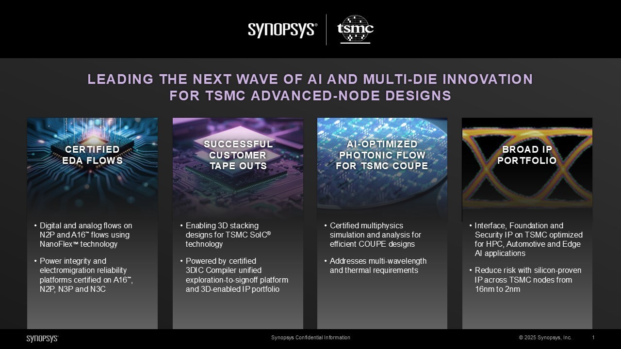
Synopsys and TSMC Drive AI Chip Innovation with Advanced EDA and IP
Insights: Synopsys continues to strengthen its partnership with TSMC to advance semiconductor innovation focused on AI and multi-die designs. Leveraging TSMC’s leading-edge processes such as N2P, A16, and future A14, Synopsys provides certified analog and digital EDA flows that optimize chip performance, power efficiency, and scalability. Their 3DIC Compiler platform supports complex 3D integration technologies…