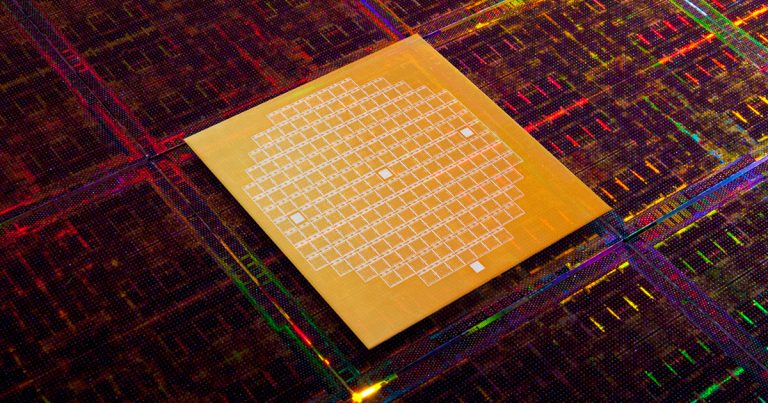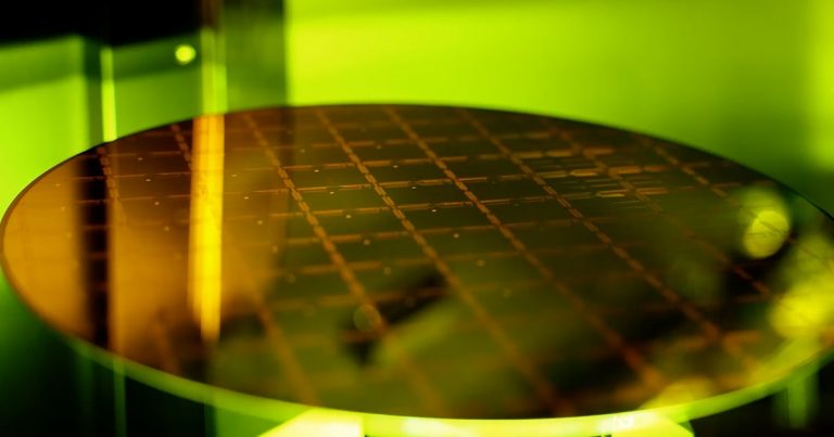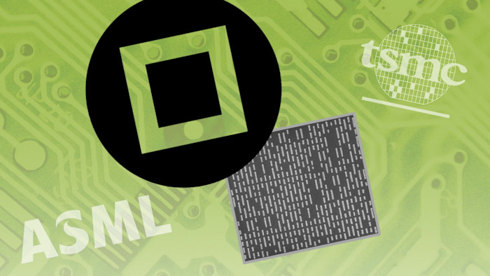
Silicon Valley start-up Substrate has announced securing over $100 million in funding, elevating its valuation to over $1 billion. The funds are earmarked for the development of particle accelerator technology for X-ray lithography in semiconductor manufacturing, a process that could alter the current economic paradigms dominated by industry titans ASML.
Key Highlights
- Substrate’s innovative approach is a reaction to global semiconductor supply chain vulnerabilities.
- Investors are willing to bet on high risks due to potential strategic implications for US tech independence.
- Cutting-edge resolution alignment with industry leaders like ASML, if verified, positions Substrate as a formidable competitor.
- Achieving cost-effective chip production could dramatically alter financial models for tech hardware companies.
The announcement underscores a significant shift in the semiconductor industry, where high production costs and reliance on a few key players have long been barriers. Substrate’s innovation, if successful, could reduce the cost of leading-edge wafer production, a goal that has attracted noteworthy investors such as Founders Fund and General Catalyst. Particularly notable is the growing desire for a robust US-based semiconductor infrastructure amid international supply chain concerns.
Substrate’s proposed technology aims to match ASML’s latest EUV tools in resolution, promising an alternative pathway that could disrupt existing manufacturing hierarchies. However, such claims warrant scrutiny given the inherent challenges in semiconductor fabrication, which include not only the technical complexities but also financial and logistical hurdles.
The successful execution of Substrate’s plan could have widespread implications, potentially reducing dependence on foreign manufacturers and bolstering America’s chipset autonomy. This aligns with strategic interests from companies like AMD and Qualcomm, potentially positioning Substrate as a key player if they can navigate the sector’s incumbent challenges.
Looking forward, Substrate’s ability to progress in research and development and secure additional strategic partnerships will be crucial. High initial and operational costs, alongside the founders’ limited experience in direct manufacturing, present critical risks. Continued funding efforts and proof of technological effectiveness will determine whether Substrate can firmly anchor itself in the competitive semiconductor landscape over the next 12 months.
How Particle Accelerator helps make chips?
How It Works?
- Electron Acceleration: An electron gun shoots a beam of electrons, which a linear accelerator (linac) accelerates to near the speed of light. [1]
- Magnetic Wiggling: The high-speed electron beam passes through an undulator, which is a track of alternating magnets. [1, 2]
- Photon Emission: As the magnets force the electrons to follow a wavy, sinusoidal path, the electrons shed energy in the form of highly coherent 13.5nm EUV photons. [1, 2]
Story by EDA Times Staff.