Insights:
- TSMC introduced the A13 process, a shrink of the A14 node, offering 6% area savings and improved efficiency.
- The A13 process maintains full backward compatibility with the A14, easing design migration for customers.
- Targeted for production in 2029, A13 aims to enhance performance and power efficiency for AI, HPC, and mobile applications.
- The announcement was made at TSMC’s 2026 North America Technology Symposium, emphasizing “Expanding AI with Leadership Silicon.”
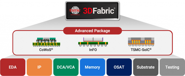
- Additional innovations include TSMC 3DFabric® advanced packaging, automotive and robotics technologies, and specialty processes.
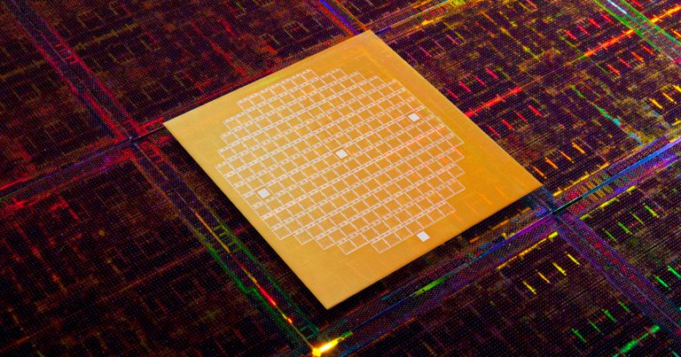
TSMC has unveiled its latest semiconductor process technology, the A13 node, at the 2026 North America Technology Symposium held in Santa Clara, California. This new process is a direct shrink of the previously announced A14 node, delivering a 6% reduction in chip area, which translates to more compact and efficient designs. These improvements primarily target the growing computational demands of next-generation artificial intelligence, high-performance computing (HPC), and mobile devices.
The A13 process offers fully backward-compatible design rules with A14, allowing customers to seamlessly transition their designs to this newest nanosheet transistor technology. Slated to enter high-volume production in 2029, one year after A14, the A13 enhances power efficiency and overall performance through comprehensive design-technology co-optimization. The launch reflects TSMC’s sustained commitment to innovation and providing reliable, leading-edge silicon technologies to support their customers’ evolving needs.
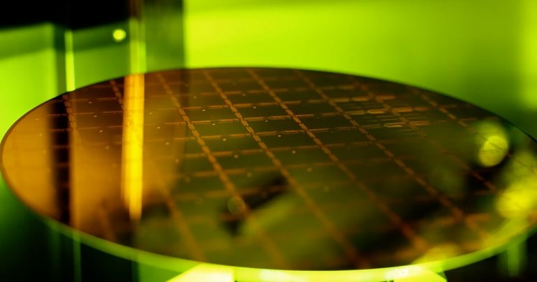
Alongside the A13 process, TSMC’s symposium highlighted other advanced technologies, including the 3DFabric® advanced packaging and 3D silicon stacking, as well as specialized automotive and robotics technologies. This annual customer-focused event showcases TSMC’s leadership in semiconductor manufacturing and ongoing efforts to drive innovation in key technology sectors.
Note: All images and Products & Trademarks mentioned in this article are copyrighted to companies:
TSMC