tsmc

  • Cadence and TSMC Forge AI Chip Design Breakthroughs

    Cadence and TSMC Forge AI Chip Design Breakthroughs

    Insights:

     Cadence and TSMC advance AI and HPC chip design with AI-driven automation and IP.

    Support for TSMC’s latest process nodes including N3, N2, A16, and upcoming A14 PDK.

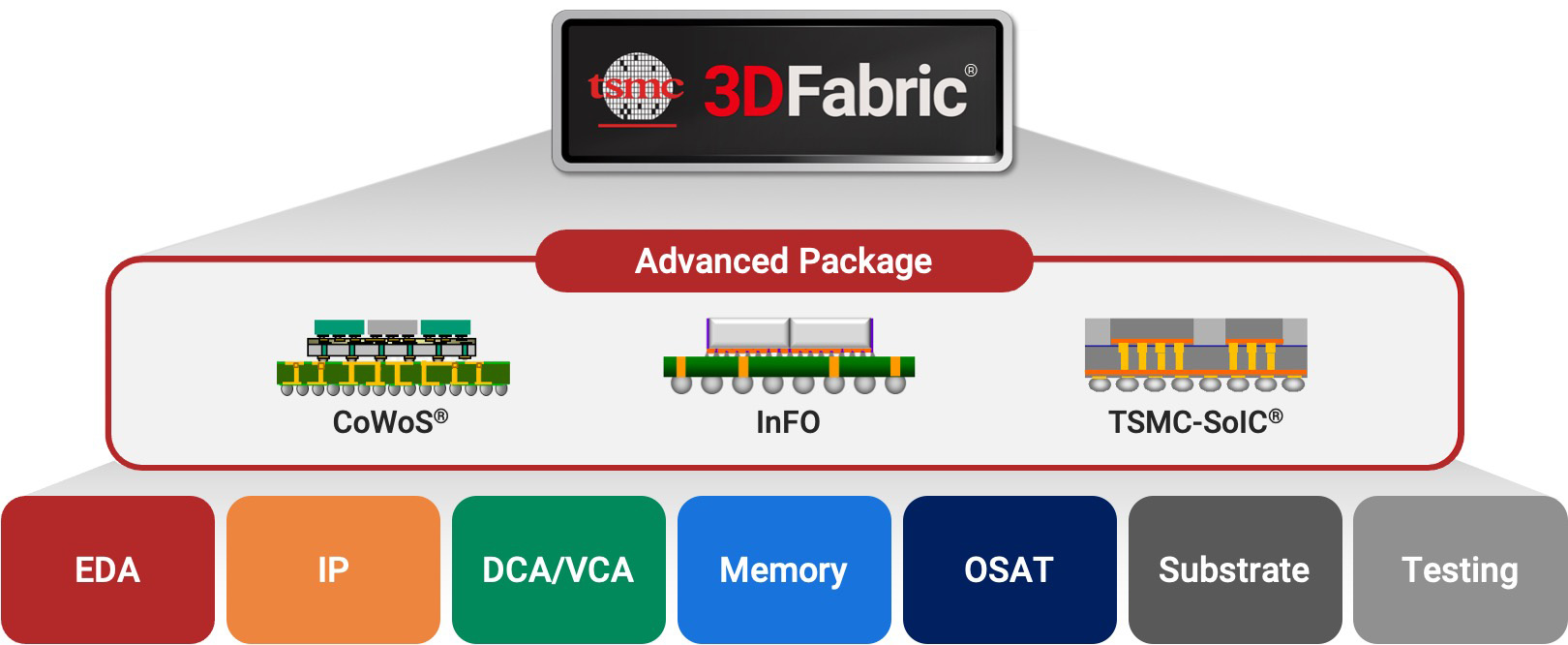
    Enhanced 3D-IC design productivity enabled by Cadence solutions integrated with TSMC’s 3DFabric.

    New silicon-proven IP such as HBM4, LPDDR6/5X, PCIe 7.0, and Universal Chiplet Interconnect for AI workloads.

    Partnership accelerates design-to-silicon journey, boosting performance and energy efficiency for next-gen semiconductors.


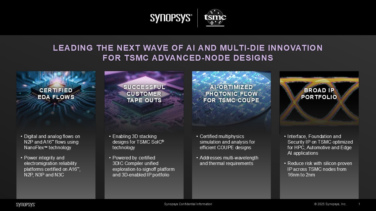
    Cadence Design Systems and TSMC continue to strengthen their partnership, delivering significant advancements in chip design automation and intellectual property (IP) to meet the demands of AI and high-performance computing (HPC) applications. Their collaboration encompasses support for the latest advanced process nodes including TSMC’s N3, N2, A16™, and upcoming A14 process technologies, leveraging AI-driven Electronic Design Automation (EDA) tools to optimize power, performance, and area.

    Cadence’s AI-powered design flows and tools like Innovus Implementation System, Cerebrus Intelligent Chip Explorer, and Clarity 3D Solver enhance productivity in complex chip and 3D-IC designs. Notably, integration with TSMC’s 3DFabric packaging technology and Compact Universal Photonic Engine facilitates system-level simulation and thermal management innovations.

    The two companies have also introduced cutting-edge silicon-proven IP on TSMC’s N3P node, including high-speed memory interfaces such as HBM4 and LPDDR6/5X, PCI Express 7.0 IP, and Universal Chiplet Interconnect (UCIe) IP. These developments are critical for addressing AI infrastructure challenges like memory bandwidth and energy-efficient scalability. Overall, this partnership empowers semiconductor customers to accelerate innovation and deploy advanced AI chips faster and more efficiently.

    For more information visit

    Note: All images and Products & Trademarks mentioned in this article are copyrighted to companies:

    Cadence Design Systems, TSMC, PCI-SIG, UCIe Consortium

  • Synopsys and TSMC Drive AI Chip Innovation with Advanced EDA and IP

    Synopsys and TSMC Drive AI Chip Innovation with Advanced EDA and IP

    Insights:

    • Synopsys and TSMC collaborate on cutting-edge multi-die AI chip designs using advanced EDA flows and IP solutions.
    • The 3DIC Compiler platform supports TSMC’s 3D packaging technologies, enabling faster tape-outs and greater design productivity.
    • Certified Synopsys digital and analog EDA tools are optimized for TSMC’s N2P, A16, and upcoming A14 processes.
    • Synopsys delivers comprehensive IP portfolios supporting high-performance standards like HBM4, PCIe 7.0, and automotive-grade IP for TSMC’s advanced nodes.
    • Collaboration extends into silicon photonics and advanced packaging technologies, enhancing multi-die integration and energy-efficient AI chip performance.

    Synopsys continues to strengthen its partnership with TSMC to advance semiconductor innovation focused on AI and multi-die designs. Leveraging TSMC’s leading-edge processes such as N2P, A16, and future A14, Synopsys provides certified analog and digital EDA flows that optimize chip performance, power efficiency, and scalability. Their 3DIC Compiler platform supports complex 3D integration technologies like SoIC and CoWoS, enabling faster design cycles and improved productivity for multi-die chip solutions.

    Additionally, Synopsys offers an extensive portfolio of IP solutions crafted for TSMC’s advanced nodes, including cutting-edge interfaces such as PCIe 7.0 and HBM4, as well as automotive-grade IP for safety-critical applications. This combined effort ensures that customers can deliver differentiated AI chips that meet stringent performance and reliability requirements while minimizing power consumption. Further collaboration in silicon photonics demonstrates their commitment to pushing the boundaries of system performance in multi-die and AI applications.

    Through this ongoing partnership, Synopsys and TSMC enable semiconductor companies to accelerate time to market and push innovation in AI-driven and multi-die integrated circuit designs, making them key enablers of the next generation of advanced semiconductor technology.

    For more information visit

    All images and Products & Trademarks mentioned in this article are copyrighted to companies involved:

    Synopsys, TSMC