Insights
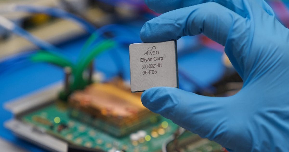
- Eliyan has successfully taped out its NuLink PHY using Samsung’s SF4X 4nm advanced manufacturing process.
- The interconnect supports up to 40Gbps bandwidth with industry-leading low power density and advanced packaging technology.
- NuLink PHY enables custom High Bandwidth Memory (HBM) base dies and supports ASIC disaggregation for chiplet-based designs.
- This technology addresses critical memory and IO bottlenecks in next-generation AI and GenAI systems.
- Collaboration with Samsung Foundry highlights the integration of advanced logic and memory technologies for data center applications.
Eliyan Corporation has announced a major breakthrough with the successful tape out of its NuLink PHY in a x64 UCIe Advanced Package Module, manufactured using Samsung Foundry’s cutting-edge SF4X 4nm process. This new chiplet interconnect technology boasts an impressive 40Gbps bandwidth at remarkably low power levels, achieving unprecedented power density through the use of 45-micron pitch micro bumps. Fully compliant with the UCIe standard, NuLink PHY extends high-performance die-to-die and die-to-memory connectivity in both standard and advanced packaging formats.
Designed to enable next-generation multi-die semiconductor architectures, Eliyan’s solution supports the creation of custom High Bandwidth Memory (HBM) base dies and is available as IP to facilitate ASIC disaggregation strategies. This addresses the critical memory and IO challenges faced by AI and GenAI subsystems, particularly in training and inference applications for large language models and other high-performance computing tasks. The collaboration with Samsung Electronics reinforces the strategic importance of integrating advanced process technology with innovative interconnect design to meet the growing demands of data centers worldwide.
Eliyan Corporation, Samsung Electronics, Samsung Foundry