Key Highlights & Insights
- NVIDIA cuLitho optimizes computational lithography using GPUs for a 40X performance improvement, drastically outpacing CPU-based methods.
- The technology addresses current challenges in semiconductor miniaturization, offering new capabilities in subatomic modeling and advanced photomask creation.
- Industry leaders like ASML, Synopsys, and TSMC are incorporating cuLitho into their workflows to significantly cut down on computational costs and energy use.
- By moving from CPUs to GPUs, cuLitho not only enhances performance but also reduces infrastructure space and power needs.
- Future advancements in chip design depend on efficient computational lithography, making NVIDIA's investment in cuLitho a strategic move for the semiconductor industry.
Introduction
If you’re elbow-deep in the world of electronic design automation (EDA) or chip design, you already know that shrinking silicon feature sizes come with staggering challenges. With every advance, computational lithography demands more—more precision, more compute power, more everything. That’s where NVIDIA’s cuLitho steps in, offering a fresh take on speeding up this critical process with GPUs. What does that mean for the industry? A quantum leap forward in efficiency that’s not just impressive on paper but viable in practice. And the best part? It’s got the backing of industry heavyweights like ASML, Synopsys, and TSMC.
Why Computational Lithography is a Big Deal
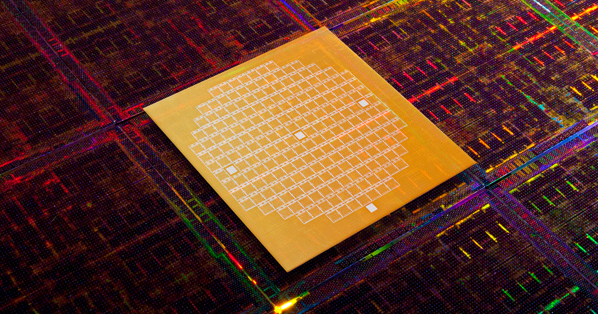
If you think about it, the whole chip-in-your-pocket revolution is built on computational lithography. It’s the process that takes complex design patterns and translates them onto silicon wafers with nano-scale precision. Think of it as painting a masterpiece, only at the atomic level and with zero room for error. The step is so compute-intensive that it constitutes a major workload for large data centers globally. NVIDIA’s cuLitho library aims to tackle this massive computational challenge head-on, moving from CPU-based methods to the high-octane world of GPUs.
The Problem: Why the Industry Needs cuLitho
As chips get smaller, optical diffraction complicates matters. To get around this, you need techniques like optical proximity correction (OPC) or inverse lithography technology (ILT) to perfect those mask patterns. The demand for these solutions grows as we push the boundaries of silicon miniaturization. But here’s the kicker: the existing infrastructure just can’t keep up—unless it upgrades how fast and efficiently it computes. Hence, every minute saved could translate into vast power savings and productivity gains.
What cuLitho Offers: Not Just Speed, but Efficiency
Let’s dig into the perks, shall we? cuLitho touts a 40X speedup in inverse lithography technology, reducing photomask processing from two weeks to overnight. Just imagine cranking out 3 to 5 times more masks daily. It achieves this by using NVIDIA GPU systems, clearly outdoing traditional 40,000 CPU systems with just 1/8th the physical space needed. We’re not just talking about moving the needle; we’re talking about flipping the dial.
Scaling for the Future
Future scaling will require new lithography innovations, and cuLitho is well-positioned to tackle what comes next—be it subatomic modeling or high-numerical aperture extreme-ultraviolet lithography. By providing a solution that’s efficient and scalable, NVIDIA ensures that companies can keep churning out increasingly advanced chips without being bogged down by escalating computational costs.
Collaborative Efforts and Industry Validation
One of the most telling endorsements of cuLitho’s potential comes from its launch partners. ASML plans on integrating GPU support across its software suite, while Synopsys collaborates with NVIDIA and TSMC to power through the complexity of advanced nodes. TSMC is already moving cuLitho into production, attesting to the dramatic improvements in performance and power efficiency. It’s not just software; it’s a collaborative edge.
Conclusion
With NVIDIA’s cuLitho, we’re not just seeing a faster, more efficient computational lithography process; we’re witnessing a foundational change in how semiconductor manufacturing will evolve. EDA Times is keeping an eye on how this technology will affect end-users, and you can bet this is just one chapter in a larger story of technological advancement. These major industry players know a good thing when they see it, and cuLitho seems to be the very thing that couldn’t have come at a better time.
Report compiled by EDA Editorial Desk. Content and images sourced from original announcements published by NVIDIA-1. This analysis constitutes transformative, educational news aggregation.