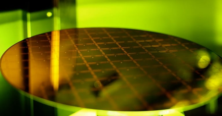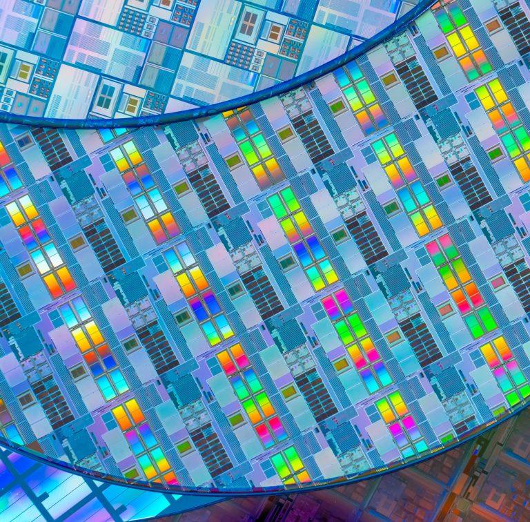
Intel Foundry has announced the general availability of the Intel 14A Process Design Kit (PDK) 0.9, marking an important development for semiconductor design. This announcement introduces a more mature design environment that provides silicon-backed validation, often crucial for customers initiating their design processes.
Key Highlights
- PDK 0.9 serves as a critical milestone for starting designs with the 14A node.
- Intel’s focus on silicon-validated PDK aligns with efforts to gain trust as a newer foundry player.
- Technologies like RibbonFET 2 and PowerDirect could be pivotal if supported by ecosystem-ready flows.
- The Q1 2027 target for PDK 1.0 sets clear expectations for stakeholders on Intel's timeline.
- Early supplier engagement and DTCO suggest alignment with industry best practices.
- Intel’s update lacks specific performance and yield data, requiring cautious optimism from investors and partners.
The Intel 14A represents a significant evolution in Intel’s process technology, building upon its predecessor, the Intel 18A. Key innovations include the use of RibbonFET 2 gate-all-around transistors, PowerDirect backside power delivery, and Turbo Cells, positioning this node as a promising candidate for advanced logic design. The PDK 0.9 also aligns with industry-standard performance claims, but Intel has not yet provided quantifiable data.
In response to market demand for enhanced design and verification environments, Intel has enlisted major electronic design automation (EDA) companies such as Synopsys, Cadence, Siemens, and Keysight, which have certified their tools to work with the 14A PDK since earlier this year. Notably, Cadence and Intel are collaborating through Design Technology Co-Optimization (DTCO) to adapt Intel 14A for AI-driven design methodologies.
The competitive landscape in semiconductor foundry services could see shifts if Intel’s momentum with PDK 0.9 translates into customer design wins. However, the real test will be reaching the PDK 1.0 milestone set for the first quarter of 2027. This milestone is expected to clear the path for high-volume manufacturing readiness.
Looking forward, the industry will be watching Intel’s progress closely. The announced timeline for PDK 1.0 presents both an opportunity and a risk. On one hand, successful adherence to the schedule could bolster Intel’s credibility and appeal among fabless design houses. On the other, any delays might impact customer confidence and strategic roadmaps. For now, Intel is leveraging enhanced inline detection and simulation practices to improve yield learning and variability control.
The upcoming months will likely see continued refinement of the Intel 14A PDK, expanded EDA/IP certifications, and deeper collaborations with suppliers. As fabless firms consider committing designs to this platform, the broader adoption of Intel 14A hinges on consistent execution and ecosystem readiness.
Story by EDA Times Staff. Originally reported by Intel.