Viz R.

  • Event: OCP Leading the Future of AI: Innovations at the 2025 OCP Global Summit

    Event: OCP Leading the Future of AI: Innovations at the 2025 OCP Global Summit

    Insights:

    • The 2025 OCP Global Summit focuses on driving AI data center innovation through openness, efficiency, sustainability, and scalability.
    • AI workloads require rethinking data center infrastructure including chiplet technology, cooling, power, networking, and systems management.
    • Edge computing for AI inference demands smaller, high-performance equipment and ultra-low latency optical networks.
    • Sustainability, particularly reducing power, water consumption, and carbon emissions, is a critical priority for future data center design.
    • The OCP AI HW/SW Co-Design group’s promotion to an official OCP Server Project signifies growing maturity and industry commitment.

    The 2025 Open Compute Project (OCP) Global Summit, themed “Leading the Future of AI,” highlights ongoing collaborations within the OCP community aimed at shaping the future of AI data centers. As AI rapidly transforms industries and economies, there is unprecedented demand for scalable, efficient, and sustainable data center infrastructure. The summit brings together global leaders to share innovations, standardize technologies, and foster partnerships that support this AI-driven evolution.

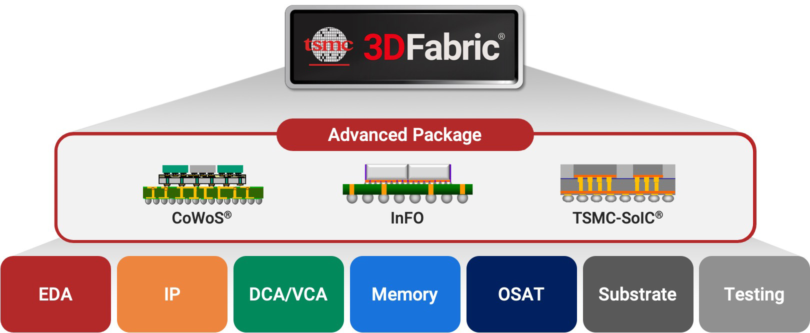
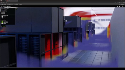
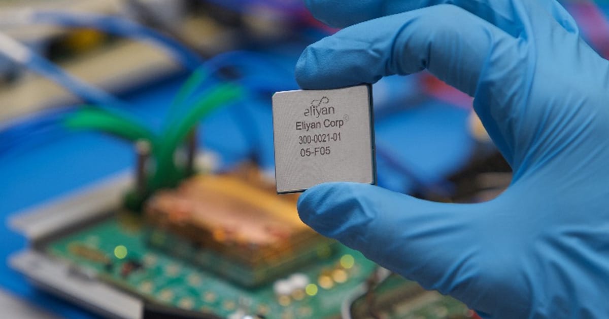
    Key advancements include breakthroughs in chiplet technologies, advanced packaging, and critical subsystems like cooling, power distribution, networking, and server architectures. The shift toward edge computing for AI inference calls for compact yet powerful computational resources combined with high-speed, low-latency optical communication networks. Sustainability remains a major focus, with ongoing efforts to reduce energy consumption, water usage, and carbon footprint within data center facilities.

    Additionally, the elevation of the AI Hardware/Software Co-Design group from a Future Technologies Initiative to an official OCP Server Project underlines the growing importance of integrated AI infrastructure development. Hosted by Rackspace and originally founded by Meta (formerly Facebook), the OCP community continues to lead in openness and innovation, paving the way for next-generation AI data centers worldwide.

    For more information visit

    Note: All images and Products & Trademarks mentioned in this article are copyrighted to companies:

    Meta, Rackspace

  • Cadence and TSMC Forge AI Chip Design Breakthroughs

    Cadence and TSMC Forge AI Chip Design Breakthroughs

    Insights:

     Cadence and TSMC advance AI and HPC chip design with AI-driven automation and IP.

    Support for TSMC’s latest process nodes including N3, N2, A16, and upcoming A14 PDK.

    Enhanced 3D-IC design productivity enabled by Cadence solutions integrated with TSMC’s 3DFabric.

    New silicon-proven IP such as HBM4, LPDDR6/5X, PCIe 7.0, and Universal Chiplet Interconnect for AI workloads.

    Partnership accelerates design-to-silicon journey, boosting performance and energy efficiency for next-gen semiconductors.


    Cadence Design Systems and TSMC continue to strengthen their partnership, delivering significant advancements in chip design automation and intellectual property (IP) to meet the demands of AI and high-performance computing (HPC) applications. Their collaboration encompasses support for the latest advanced process nodes including TSMC’s N3, N2, A16™, and upcoming A14 process technologies, leveraging AI-driven Electronic Design Automation (EDA) tools to optimize power, performance, and area.

    Cadence’s AI-powered design flows and tools like Innovus Implementation System, Cerebrus Intelligent Chip Explorer, and Clarity 3D Solver enhance productivity in complex chip and 3D-IC designs. Notably, integration with TSMC’s 3DFabric packaging technology and Compact Universal Photonic Engine facilitates system-level simulation and thermal management innovations.

    The two companies have also introduced cutting-edge silicon-proven IP on TSMC’s N3P node, including high-speed memory interfaces such as HBM4 and LPDDR6/5X, PCI Express 7.0 IP, and Universal Chiplet Interconnect (UCIe) IP. These developments are critical for addressing AI infrastructure challenges like memory bandwidth and energy-efficient scalability. Overall, this partnership empowers semiconductor customers to accelerate innovation and deploy advanced AI chips faster and more efficiently.

    For more information visit

    Note: All images and Products & Trademarks mentioned in this article are copyrighted to companies:

    Cadence Design Systems, TSMC, PCI-SIG, UCIe Consortium

  • Synopsys and GlobalFoundries launch a global pilot program offering a ‘chip design to tapeout’ curriculum to universities.

    Insights:

    • Synopsys and GlobalFoundries launch a global pilot program offering a ‘chip design to tapeout’ curriculum to universities.
    • Over 40 universities worldwide participate, gaining access to professional-grade EDA tools and advanced manufacturing capabilities.
    • The program bridges academia and industry by enabling students to design and fabricate real silicon chips affordably.
    • Training for professors and comprehensive course content are integral to embedding hands-on chip design into academic curricula.
    • This initiative supports workforce development and accelerates semiconductor innovation by cultivating practical engineering skills.

    Synopsys and GlobalFoundries have partnered to introduce a pioneering educational program aimed at equipping university students with practical experience in chip design and fabrication. This pilot initiative, launching at over 40 universities worldwide, provides students and professors with professional-grade electronic design automation (EDA) tools from Synopsys and access to manufacturing through GlobalFoundries’ multi-project wafer program. By significantly lowering the cost barriers associated with custom silicon production, the program allows students to transform design concepts into tangible silicon chips.

    The collaboration goes beyond providing tools; it includes training professors to lead hands-on courses and offers detailed curriculum support. This integrated approach bridges theoretical learning with real-world semiconductor processes, fostering a deeper understanding and skillset for the next generation of engineers. The program exemplifies a commitment to semiconductor workforce development and academic-industry collaboration, addressing critical skill gaps while accelerating innovation.

    GlobalFoundries’ University Partnership Program amplifies this effort by aligning research projects with cutting-edge semiconductor technologies, further enriching the educational experience. Together, Synopsys and GlobalFoundries are shaping the future of chip design education and empowering talented students to contribute meaningfully to the semiconductor industry’s evolving landscape.

    For more information visit

    Note: All images and Products & Trademarks mentioned in this article are copyrighted to companies:

    Synopsys, Inc., GlobalFoundries

  • Synopsys and TSMC Drive AI Chip Innovation with Advanced EDA and IP

    Synopsys and TSMC Drive AI Chip Innovation with Advanced EDA and IP

    Insights:

    • Synopsys and TSMC collaborate on cutting-edge multi-die AI chip designs using advanced EDA flows and IP solutions.
    • The 3DIC Compiler platform supports TSMC’s 3D packaging technologies, enabling faster tape-outs and greater design productivity.
    • Certified Synopsys digital and analog EDA tools are optimized for TSMC’s N2P, A16, and upcoming A14 processes.
    • Synopsys delivers comprehensive IP portfolios supporting high-performance standards like HBM4, PCIe 7.0, and automotive-grade IP for TSMC’s advanced nodes.
    • Collaboration extends into silicon photonics and advanced packaging technologies, enhancing multi-die integration and energy-efficient AI chip performance.

    Synopsys continues to strengthen its partnership with TSMC to advance semiconductor innovation focused on AI and multi-die designs. Leveraging TSMC’s leading-edge processes such as N2P, A16, and future A14, Synopsys provides certified analog and digital EDA flows that optimize chip performance, power efficiency, and scalability. Their 3DIC Compiler platform supports complex 3D integration technologies like SoIC and CoWoS, enabling faster design cycles and improved productivity for multi-die chip solutions.

    Additionally, Synopsys offers an extensive portfolio of IP solutions crafted for TSMC’s advanced nodes, including cutting-edge interfaces such as PCIe 7.0 and HBM4, as well as automotive-grade IP for safety-critical applications. This combined effort ensures that customers can deliver differentiated AI chips that meet stringent performance and reliability requirements while minimizing power consumption. Further collaboration in silicon photonics demonstrates their commitment to pushing the boundaries of system performance in multi-die and AI applications.

    Through this ongoing partnership, Synopsys and TSMC enable semiconductor companies to accelerate time to market and push innovation in AI-driven and multi-die integrated circuit designs, making them key enablers of the next generation of advanced semiconductor technology.

    For more information visit

    All images and Products & Trademarks mentioned in this article are copyrighted to companies involved:

    Synopsys, TSMC

  • Siemens and ASE Revolutionize 3D Semiconductor Packaging with Innovator3D IC

    Insights:

    • Siemens Digital Industries Software partners with ASE to advance 3Dblox workflows for ASE’s VIPack™ platform.
    • The collaboration focuses on Fanout Chip-on-Substrate, FOCoS-Bridge, and TSV-based 2.5D/3D IC packaging technologies.
    • The partnership accelerates design flexibility, package innovation, and time-to-market for complex chiplet-based integration.
    • Siemens’ Innovator3D IC solution is fully certified for 3Dblox, enabling efficient package design and verification.
    • 3Dblox and Innovator3D IC enable hierarchical device planning crucial for next-generation heterogeneous integration.

    Siemens Digital Industries Software has joined forces with Advanced Semiconductor Engineering, Inc. (ASE) to develop and validate 3Dblox-based workflows for ASE’s advanced VIPack™ platform. This collaboration targets key semiconductor packaging technologies, including Fanout Chip-on-Substrate (FOCoS), FOCoS-Bridge, and Through Silicon Via (TSV)-based 2.5D and 3D ICs. Siemens’ Innovator3D IC solution, fully certified for the 3Dblox standard, acts as a rapid design assembly exploration tool that fosters interoperability and streamlines the design process.

    ASE’s VIPack platform, a next-generation heterogeneous integration architecture, supports comprehensive co-design across six core packaging pillars. It leverages advanced redistribution layer (RDL) processes and 3D technologies to achieve ultra-high density and superior performance by integrating multiple chips into one package. The collaboration enhances design flexibility and accelerates the time-to-market by allowing customers to quickly address complex packaging challenges with EDA tool compatibility.

    The partnership also emphasizes System Technology Co-optimization (STCO) through hierarchical device planning, imperative for advanced chiplet-based heterogeneous integration. Both Siemens and ASE acknowledge their ongoing commitment to 3Dblox as a foundation for semiconductor package design that delivers open interoperability and innovation for future chip packaging solutions.

    For more information visit

    Siemens Digital Industries Software, Advanced Semiconductor Engineering, Inc. (ASE)

  • onsemi Acquires Aura Semiconductor’s Vcore Power Technologies

    onsemi Acquires Aura Semiconductor’s Vcore Power Technologies

    Insights:

    • onsemi has agreed to acquire Aura Semiconductor’s Vcore power technologies and related IP licenses.
    • The acquisition strengthens onsemi’s power management portfolio for AI data center applications.
    • This move supports onsemi’s goal to provide comprehensive power solutions from grid to core for AI infrastructure.
    • Integration of Vcore tech will enhance power density, efficiency, and thermal performance in compute racks.
    • The deal is expected to close in Q4 2025 with minimal impact on near-term earnings and accretive results thereafter.

    onsemi announced on September 22, 2025, that it has entered into an agreement to acquire rights and intellectual property related to Aura Semiconductor’s Vcore power technologies. This strategic acquisition is designed to enhance onsemi’s power management solutions, particularly for AI data centers. The integration of these technologies will enable onsemi to offer a more comprehensive and differentiated power portfolio, addressing the full power spectrum from grid to core.

    Sudhir Gopalswamy, group president at onsemi, emphasized that the acquisition aligns with the company’s commitment to meeting the efficiency and energy demands of future AI data infrastructure. The new capabilities will improve power density, thermal management, and efficiency, which in turn increases computing capacity per rack. onsemi, known for its innovation in silicon and silicon carbide technologies, aims to become a leading supplier of scalable and practical power solutions for AI and modern data centers.

    The transaction, expected to close in the fourth quarter of 2025, is forecasted to have minimal impact on onsemi’s earnings per share in the first year following closing and be accretive thereafter. This acquisition reinforces onsemi’s competitive position in an evolving market focused on electrification, sustainable energy, and cloud infrastructure.

    For more information visit

    onsemi, Aura Semiconductor

  • Micron Reports Record Q4 Revenue Fueled by AI Data Center Demand

    Micron Reports Record Q4 Revenue Fueled by AI Data Center Demand

    Insights:

    • Micron Technology achieved record-breaking fiscal Q4 and full-year 2025 revenue driven by AI data center growth.
    • Capital expenditures reached $13.8 billion for the full fiscal year 2025, reflecting strong investment in future capabilities.
    • Adjusted free cash flow was $3.72 billion for fiscal 2025, supporting financial stability and shareholder returns.
    • The company declared a quarterly dividend of $0.115 per share, emphasizing its commitment to investors.
    • Micron expects $1.2 billion sequential revenue growth in Q1 2026 with gross margins exceeding 50%, highlighting strong market momentum.

    Micron Technology, Inc. closed fiscal year 2025 with record-breaking financial performance, largely driven by strong demand for AI data center memory solutions. The company’s Q4 results reinforced its leadership position in technology and operational excellence, setting the stage for continued growth into fiscal 2026. With a portfolio of high-performance DRAM, NAND, and NOR products, Micron is strategically positioned to capitalize on the growing AI market as the only U.S.-based memory manufacturer.

    During fiscal 2025, Micron made substantial capital investments totaling $13.8 billion, demonstrating its commitment to expanding its manufacturing and technological capabilities. The company generated an impressive adjusted free cash flow of $3.72 billion, which supports ongoing innovation and shareholder value initiatives, including a recently declared quarterly dividend of $0.115 per share.

    Looking ahead, Micron forecasts $1.2 billion in sequential revenue growth for the first quarter of fiscal 2026, with gross margins expected to exceed 50%. This outlook reflects solid market demand and confidence in its competitive product portfolio. Micron continues to drive innovation that enables AI, compute-intensive applications, and the broader data economy, positioning itself for sustained long-term success.

    For more information visit

    Micron Technology, Inc.

  • UK and NVIDIA Unite to Drive AI Innovation and Infrastructure

    UK and NVIDIA Unite to Drive AI Innovation and Infrastructure

    Insights:

    • NVIDIA CEO Jensen Huang highlighted the UK as a burgeoning AI ecosystem with 3,700 companies and 60,000 employees.
    • The UK-US collaboration involves the largest-ever tech agreement focusing on AI for security, innovation, and economic growth.
    • NVIDIA committed £2 billion in investments with UK-based venture capital firms to foster AI startups and scale technology impact.
    • Deployment of 120,000 NVIDIA Blackwell GPUs will power new AI “factories,” including partnerships with Microsoft, OpenAI, and others.
    • Projects include building a quantum-GPU supercenter and launching a robotics R&D hub to train the next generation of AI talent.

    This week, the United Kingdom emerged as a global AI hub during NVIDIA CEO Jensen Huang’s visit, marked by a high-profile event in London featuring UK Prime Minister Keir Starmer and senior government officials. The gathering emphasized the UK’s unique “Goldilocks moment,” where top universities, researchers, startups, and venture capital converge to create fertile ground for AI innovation. Huang praised the UK’s talented workforce and its historical significance as the birthplace of the industrial revolution, framing AI as the next major industrial leap.

    The collaboration between the UK and the US, anchored by NVIDIA’s £2 billion investment and the largest-ever deployment of 120,000 NVIDIA Blackwell GPUs, aims to bolster AI infrastructure and commercialize cutting-edge science. This investment partnership includes leading VC firms and spans several cities beyond London, underscoring a nationwide impact. Key initiatives also include developing quantum computing capabilities, launching dedicated robotics research hubs, and accelerating major AI projects in healthcare, climate science, and public services, powered by the UK’s most powerful AI supercomputer based at the University of Bristol.

    For more information visit

    NVIDIA, Accel, Air Street Capital, Balderton Capital, Hoxton Ventures, Phoenix Court, Microsoft, Nscale, OpenAI, CoreWeave, Oxford Quantum Circuits, techUK, QA, University of Bristol

  • NVIDIA and Intel Unite to Revolutionize AI and Computing Technologies

    NVIDIA and Intel Unite to Revolutionize AI and Computing Technologies

    Insights:

    • NVIDIA and Intel announce a strategic collaboration to develop custom datacenter and PC products combining their strengths.
    • Intel will create x86 CPUs customized for NVIDIA AI platforms and x86 SOCs integrating NVIDIA RTX GPU chiplets for personal computing.
    • NVIDIA commits a $5 billion investment in Intel’s common stock, solidifying their partnership.
    • This joint effort aims to seamlessly connect NVIDIA’s AI and accelerated computing with Intel’s CPU technologies and x86 ecosystem.
    • Both companies emphasize innovation to drive the next era of computing across hyperscale, enterprise, and consumer markets.

    NVIDIA and Intel have announced a groundbreaking collaboration to jointly develop next-generation custom datacenter and personal computing products that combine their technological expertise. This partnership will leverage NVIDIA’s powerful AI and accelerated computing platforms alongside Intel’s leading x86 CPUs and architecture. Intel plans to build NVIDIA-customized x86 CPUs specifically for integration into NVIDIA’s AI infrastructure, while for personal computers, Intel will design x86 system-on-chips (SOCs) incorporating NVIDIA RTX GPU chiplets.

    As part of this strategic alliance, NVIDIA also plans to invest $5 billion in Intel’s common stock, underscoring the deep commitment between the two tech giants. The companies aim to seamlessly connect their architectures via NVIDIA’s NVLink technology to provide innovative solutions across hyperscale data centers, enterprises, and consumer markets. Both CEOs highlight this as a pivotal step in advancing computing by merging their strengths and expanding their ecosystems for future workloads and AI-driven applications.

    For more information visit

    NVIDIA, Intel Corporation

  • Cadence Boosts SoC Design Power with Arm Artisan IP Acquisition

    Cadence Boosts SoC Design Power with Arm Artisan IP Acquisition

    Insights

    • Cadence has acquired Arm’s Artisan foundation IP business, expanding its design IP portfolio.
    • The acquisition includes standard cell libraries, memory compilers, and GPIOs optimized for advanced foundries.
    • This move supports Cadence’s strategy to improve time-to-market, cost, power, and performance for SoC designs.
    • The acquisition is expected to have minimal impact on Cadence’s revenue and earnings in 2025.
    • Cadence continues to lead in AI-driven semiconductor design solutions and was recently named a top-managed company by the Wall Street Journal.

    Cadence Design Systems has completed the acquisition of the Arm Artisan foundation IP business, a significant addition to its expanding suite of semiconductor design solutions. The acquired IP includes critical components such as standard cell libraries, memory compilers, and general-purpose I/Os—elements optimized for advanced semiconductor process nodes used by leading foundries.

    This strategic move enhances Cadence’s presence in system-on-chip (SoC) design by complementing its existing portfolio of protocol, interface, memory, and SerDes IPs. By integrating the Artisan IP, Cadence aims to accelerate customers’ time to market while optimizing cost, power efficiency, and performance in next-generation chip designs.

    While the acquisition will not meaningfully affect Cadence’s financial results in the near term, it reinforces the company’s commitment to innovation and leadership in AI-driven system design solutions. Cadence’s strong market position is further validated by its recognition as one of the world’s best-managed companies. This acquisition positions Cadence to better serve a diverse range of industries such as mobile communications, automotive, aerospace, and more.

    Cadence, Arm

    For more information visit

  • Eliyan’s NuLink PHY Advances High-Performance Chiplet Interconnects

    Eliyan’s NuLink PHY Advances High-Performance Chiplet Interconnects

    Insights

    • Eliyan has successfully taped out its NuLink PHY using Samsung’s SF4X 4nm advanced manufacturing process.
    • The interconnect supports up to 40Gbps bandwidth with industry-leading low power density and advanced packaging technology.
    • NuLink PHY enables custom High Bandwidth Memory (HBM) base dies and supports ASIC disaggregation for chiplet-based designs.
    • This technology addresses critical memory and IO bottlenecks in next-generation AI and GenAI systems.
    • Collaboration with Samsung Foundry highlights the integration of advanced logic and memory technologies for data center applications.

    Eliyan Corporation has announced a major breakthrough with the successful tape out of its NuLink PHY in a x64 UCIe Advanced Package Module, manufactured using Samsung Foundry’s cutting-edge SF4X 4nm process. This new chiplet interconnect technology boasts an impressive 40Gbps bandwidth at remarkably low power levels, achieving unprecedented power density through the use of 45-micron pitch micro bumps. Fully compliant with the UCIe standard, NuLink PHY extends high-performance die-to-die and die-to-memory connectivity in both standard and advanced packaging formats.

    Designed to enable next-generation multi-die semiconductor architectures, Eliyan’s solution supports the creation of custom High Bandwidth Memory (HBM) base dies and is available as IP to facilitate ASIC disaggregation strategies. This addresses the critical memory and IO challenges faced by AI and GenAI subsystems, particularly in training and inference applications for large language models and other high-performance computing tasks. The collaboration with Samsung Electronics reinforces the strategic importance of integrating advanced process technology with innovative interconnect design to meet the growing demands of data centers worldwide.

    For more information visit

    Eliyan Corporation, Samsung Electronics, Samsung Foundry

  • Keysight and Intel Unveil Advanced Chiplet Solutions for AI & Data Centers

    Insights

    • Keysight and Intel Foundry collaborate to advance EMIB-T technology for AI and data center chips.
    • Adoption of open standards like UCIe™ 2.0 and BoW ensures seamless chiplet interoperability.
    • Keysight’s Chiplet PHY Designer offers pre-silicon validation to streamline chiplet design and reduce risks.
    • The partnership accelerates innovation by enabling faster, more reliable high-performance semiconductor packaging.
    • Demonstrations of the new EMIB-T workflow are showcased at Intel Foundry Direct Connect event.

    Keysight Technologies and Intel Foundry have announced a strategic collaboration to support Embedded Multi-die Interconnect Bridge-T (EMIB-T) technology, a breakthrough packaging solution tailored for the demanding AI and data center markets. This partnership addresses the critical need for reliable, high-speed communication and efficient power delivery between chiplets and 3D integrated circuits, which are essential for next-generation semiconductor performance.

    By leveraging emerging open standards such as Universal Chiplet Interconnect Express™ (UCIe™) 2.0 and Bunch of Wires (BoW), Keysight and Intel aim to create a robust chiplet interoperability ecosystem. Keysight’s Chiplet PHY Designer now integrates advanced simulation and validation capabilities aligned with these standards, offering engineers a streamlined, pre-silicon design verification process that reduces development costs and mitigates manufacturing risks.

    This collaboration enhances chiplet design flexibility, empowering rapid innovation and ensuring customers can meet future workloads with precision. The advanced EMIB-T workflow will be showcased by Keysight at the Intel Foundry Direct Connect event, highlighting this pivotal step in semiconductor packaging technology.

    For more information visit