The semiconductor industry is undergoing a seismic shift, and two technology powerhouses are leading the charge. Cadence, a recognized leader in AI-driven computational software for semiconductor and system design, has announced a strategic collaboration with Google to bring its ChipStack AI Super Agent to Google Cloud — powered by Google’s cutting-edge Gemini models. The result is a cloud-native, agent-driven platform poised to redefine how chips are designed and verified.
At its core, the collaboration integrates Cadence’s ChipStack AI Super Agent with Gemini’s large language model (LLM) reasoning capabilities, creating a tightly coupled solution that targets some of the most time-consuming and complex tasks in chip development. According to Cadence, the platform delivers up to 10X productivity improvements across key workflows, including digital design, testbench development, verification planning, regression management, and automated debug.
What makes ChipStack stand out is its proprietary Mental Model technology. Rather than simply generating code or suggestions, the system applies sophisticated agentic reasoning through Cadence-native skills, actively driving Cadence EDA tools to improve the quality and correctness of LLM-generated content. This is not AI as a passive assistant — it is AI as an active collaborator in the design process.
“Our collaboration with Google Cloud represents a major step forward in scaling AI-driven design automation,” said Paul Cunningham, Senior Vice President and General Manager at Cadence. “By integrating the Cadence ChipStack AI Super Agent with Gemini, we’re advancing the next generation of agentic design — combining the reasoning power of large language models with Cadence’s world-class EDA engines to deliver breakthrough productivity and quality of results for our customers.”
The platform also capitalizes on Google Cloud’s secure, elastic compute infrastructure, which provides the computational muscle required for Gemini’s LLM reasoning, Cadence EDA tools, and the ChipStack AI Super Agent to operate in concert. This infrastructure backbone enables a streamlined “click-to-deploy” experience, meaning design teams can spin up an end-to-end, agent-powered chip design and verification environment without the friction traditionally associated with complex EDA deployments.
For engineering teams facing relentless pressure to compress development cycles and accelerate time to tapeout, this kind of deployment simplicity is more than a convenience — it is a competitive advantage. By abstracting away infrastructure complexity and embedding AI reasoning directly into proven EDA workflows, Cadence and Google are lowering the barrier for organizations to adopt agentic automation at scale.
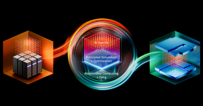
The timing of this announcement is significant. As chip designs grow increasingly complex and the global demand for custom silicon intensifies — driven by AI hardware, automotive applications, and next-generation communications — the industry needs smarter tools, not just faster ones. The ChipStack AI Super Agent addresses this need by coupling intelligent automation with deep domain expertise baked directly into Cadence’s EDA engines.
This collaboration signals a broader industry trend: the convergence of foundation model AI and specialized engineering software. Rather than treating LLMs as generic tools bolted onto existing workflows, Cadence and Google are building a purpose-built, integrated platform where AI reasoning and EDA execution are deeply intertwined.
The Cadence ChipStack AI Super Agent is available now on the Google Cloud Marketplace, offering design teams immediate access to what could become the new standard for intelligent chip design automation. For organizations looking to stay competitive in an era of increasingly complex silicon, this platform represents a compelling and timely opportunity to modernize their design methodology.