Synopsys, Inc. has unveiled its Multiphysics Fusion solutions, a development aimed at tackling the intricate physics challenges now prevalent in semiconductor design. The introduction of this integrated solution could have substantial implications for industries focused on AI and high-performance computing applications.
Key Highlights
- The partnership between Synopsys and Ansys highlights strategic collaboration to boost EDA capabilities.
- Initial validations by industry leaders suggest real-world efficacy of the Multiphysics Fusion solutions.
- The solutions could represent a shift from overdesign to co-design in the semiconductor industry.
- The industry is trending towards more unified design workflows across different domains.
- Successful integration into customer workflows will be vital for the widespread adoption and impact of these solutions.
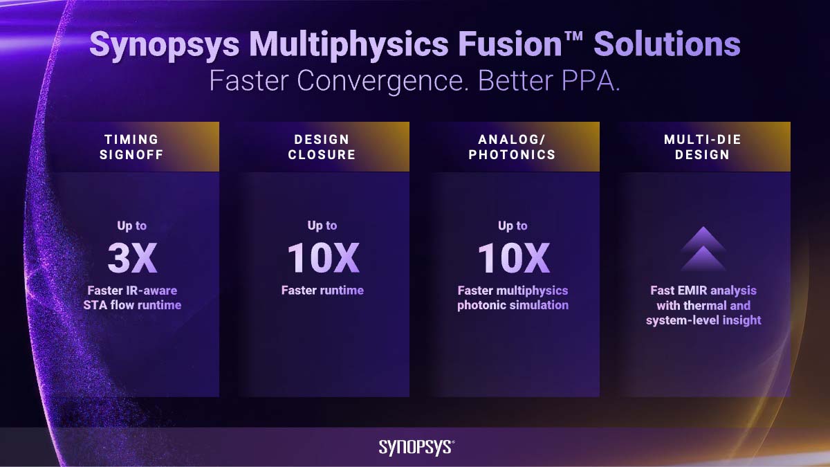
Synopsys is collaborating with key industry players like MediaTek, NVIDIA, and Samsung Electronics to validate its latest offering in operational environments. According to the company, early feedback indicates improved workflow effectiveness and substantially reduced incidents of late-stage design rework. This development may offer significant enhancements in design cycles by providing multiphysics analysis within EDA workflows, potentially reducing run times by up to threefold and expediting design closure tenfold.
This integration offers a shift towards co-design and away from traditional overdesign methods, marking a significant evolution in semiconductor design capabilities. However, the adoption of such solutions in current design schemes may not be straightforward. Companies heavily reliant on entrenched workflows could face challenges in integrating these advanced tools, an uncertainty acknowledged by Synopsys.
Story by EDA Times Staff. Originally reported by Synopsys Newsroom.