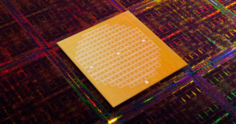
Lam Research has introduced Aether® dry resist technology, a promising development in extreme ultraviolet (EUV) lithography. This move could significantly benefit semiconductor manufacturing, particularly at advanced process nodes below 10 nanometers. Dry resist offers an efficient alternative to traditional wet resist, achieving higher resolution and reducing scanner dose requirements. By eliminating the use of perfluoroalkyl and polyfluoroalkyl substances (PFAS), acids, and solvents, this technology champions sustainability while promoting lower defect rates and energy consumption.
Key Highlights
- The shift to dry resist could improve manufacturing efficiency and reduce costs in EUV processes.
- Lam Research is positioned as a key player in next-generation lithography.
- Advancements in dry resist contribute to achieving the aggressive miniaturization targets of the semiconductor industry.
- Sustainability measures, such as avoiding PFAS, provide long-term environmental benefits.
- High adoption of dry resist could challenge existing resist market participants, pressuring them to adapt.
The semiconductor industry has been steadily advancing towards ever smaller and more efficient chips, a trend that underscores the importance of EUV lithography. As the drive for miniaturization continues, manufacturers face increasing challenges to sustain cost efficiency and environmental standards. Dry resist technology addresses both, paving the way for more sustainable practices.
Key to Lam Research’s innovation is its ability to support sub-10-nanometer patterning, enabling chipmakers to keep up with aggressive miniaturization targets. This technological feat could offer Lam Research a competitive advantage, positioning them as a crucial ally for semiconductor companies keen on adopting EUV lithography.
However, the widespread implementation of dry resist technology depends heavily on the rate at which the industry adopts EUV lithography. Potential high costs and operational changes could pose challenges for manufacturers still relying on wet resist processes.
The upcoming year presents a critical period for this technology, with anticipated growth in adoption by leading-edge chip manufacturers. The industry will be observing closely as more semiconductor companies evaluate the benefits and challenges posed by the transition to dry resist. For Lam Research, successfully navigating these dynamics could translate into enhanced market positioning as a leader in next-gen lithography solutions.
Story by EDA Times Staff. Originally reported by LAM.